
|
The printed circuit card (PCB) manufacturing procedure needs a complicated treatment to ensure the performance of the completed product. Though motherboard can be single, double or multilayered, the construction procedures used just differ after the very first layer's production. As a result of differences in the structure of the PCBs, some might need 20 or more steps during production.
The variety of actions needed for generating printed circuit card correlates to their complexity. Missing any type of step or cutting down on the treatment could negatively impact the efficiency of the circuit card. However, when effectively finished, the PCBs need to execute their jobs appropriately as crucial digital components. Printed Circuit Board Production Process WHAT ARE THE PARTS OF A PCB? There are 4 almosts all to a PCB: Substratum: The first, and also essential, is the substratum, generally made of fiberglass. Fiberglass is used since it gives a core stamina to the PCB as well as assists stand up to breakage. Think of the substratum as the PCB's "skeleton". Copper Layer: Depending upon the board kind, this layer can either be copper aluminum foil or a full-on copper covering. No matter which strategy is utilized, the factor of the copper is still the very same-- to carry electrical signals to and also from the PCB, just like your nerves lugs signals between your brain and your muscles. Solder Mask: The third piece of the PCB assembly services is the solder mask, which is a layer of polymer that assists shield the copper so that it does not short-circuit from entering contact with the atmosphere. In this way, the solder mask acts as the PCB's "skin". Silkscreen: The last part of the circuit board is the silkscreen. The silkscreen is typically on the component side of the board used to show component numbers, logos, signs switch setups, part referral and examination factors. The silkscreen can additionally be referred to as legend or nomenclature. Obtain Rates as well as Preparation The parts of PCB- silkscreen, soldermask, copper, and substratum= len. Since we have actually reviewed the fundamentals of PCBs as well as PCB makeup, we'll walk through the whole process of just how to develop a PCB. HOW IS A PCB MADE? The actions of the PCB design procedure begin with style and verification and also continue through the fabrication of the motherboard. Many actions call for computer guidance and machine-driven tools to make sure accuracy and also prevent short circuits or incomplete circuits. The completed boards have to go through stringent screening before they are packaged and also supplied to consumers. Step One: Creating the PCB. The start action of any kind of PCB manufacture is, obviously, the design. PCB manufacture as well as style always begin with a plan: the developer lays out a blueprint for the PCB that meets all the requirements as detailed. One of the most commonly-used style software application used by PCB developers is a software program called Extended Gerber-- likewise called IX274X. step one in pcb: the mostly generally used layout software application made use of by pcb designers is called prolonged gerber-also called IX274X. When it involves PCB style, Extended Gerber is an excellent item of software program due to the fact that it also works as an output style. Expanded Gerber inscribes all the details that the developer needs, such as the variety of copper layers, the variety of solder masks needed and the other items of component symbols. When a design blueprint for the PCB is encoded by the Gerber Extended software application, all the different components and elements of the design are checked over to make certain that there are no errors. As soon as the examination by the developer is total, the completed PCB layout is sent to a PCB fabrication house to ensure that the PCB can be constructed. On arrival, the PCB layout plan undergoes a second check by the maker, referred to as a Style for Manufacture (DFM) check. A proper DFM check makes certain that the PCB design fulfills, at minimum, the tolerances required for manufacture. Tip 2: Style Review and Engineering Questions. Another crucial action of the published circuit board manufacture procedure involves inspecting the design for potential errors or problems. A designer goes over every part of the PCB layout to make certain there are no missing parts or wrong structures. After getting clearance from a designer, the design moves to the printing phase. Tip Three: Publishing the PCB Design. Besides the checks are complete, the PCB layout can be printed. Unlike various other strategies, like building illustrations, PCB strategies don't publish out on a regular 8.5 x 11 sheet of paper. Rather, a special sort of printer, known as a plotter printer, is utilized. A plotter printer makes a "film" of the PCB. The final product of this "film" looks just like the transparencies that used to be made use of in schools-- it's essentially an image adverse of the board itself. The within layers of the PCB are stood for in 2 ink shades:. Black Ink: Used for the copper traces as well as circuits of the PCB. Clear Ink: Denotes the non-conductive areas of the PCB, like the fiberglass base. On the outer layers of the PCB design, this pattern is reversed-- clear ink describes the line of copper paths, yet black ink likewise describes areas where the copper will be eliminated. Each PCB layer and the going along with solder mask gets its very own film, so a basic two-layer PCB needs 4 sheets-- one for every layer and one each for the coming with solder mask. After the film is published, they're aligned and also a hole, known as an enrollment hole, is punched via them. The enrollment hole is utilized as a guide to line up the films in the future in the process. Step Four: Publishing the Copper for the Interior Layers. Step 4 is the first step in the process where the producer begins to make the PCB. After the PCB style is published onto a piece of laminate, copper is then pre-bonded to that exact same piece of laminate, which serves as the structure for the PCB. The copper is then engraved away to expose the blueprint from earlier. Next off, the laminate panel is covered by a sort of photo-sensitive movie called the withstand. The resist is constructed from a layer of photo-reactive chemicals that harden after they're revealed to ultraviolet light. The resist allows technicians to get a best match between the photos of the plan and also what's published to the photoresist. Once the resist and the laminate are lined up-- using the holes from earlier-- they receive a blast of ultraviolet light. The ultraviolet light passes through the transparent parts of the movie, hardening the photoresist. This indicates locations of copper that are indicated to be maintained as pathways. On the other hand, the black ink protects against any type of light from reaching the locations that aren't indicated to harden to make sure that they can later be removed. As soon as the board has actually been prepared, it is cleaned with an alkaline solution to get rid of any of the leftover photoresists. The board is then pressure-washed to get rid of anything left on the surface and also entrusted to completely dry. After drying out, the only withstand that need to be left on the PCB is on top of the copper that remains as part of the PCB when it's lastly stood out complimentary. A professional looks over the PCBs to make that there are no mistakes. If no errors exist, then it's on to the next action. Tip 5: Engrave the Inner Layers or Core to Get Rid Of Copper. The core or inner layers of the printed circuit card need to have added copper got rid of prior to the PCB construction procedure can continue. Etching includes covering the required copper on the board as well as subjecting the rest of the board to a chemical. The chemical etching procedure gets rid of all vulnerable copper from the PCB, leaving only the board's required quantity. This action might differ in its time or the quantity of copper etching solvent used. Big PCBs or those with larger frameworks might use a lot more copper, resulting in more copper that has to undergo etching for elimination. Consequently, these boards will certainly call for additional time or solvent. If a Printed Circuit Board Production Refine Is for Multilayer Layouts. Multilayer printed circuit boards have extra actions to make up the added layers of the style throughout their manufacture. These actions mirror many of those used throughout solitary layer PCBs. However, the phases repeat for every layer of the board. Also, in multilayer PCBs, copper foil usually changes copper finishing in between the layers. Printed Circuit Board Manufacturing Process. Internal Layer Imaging. Internal layer imaging follows the very same treatments as publishing the PCB layout. The design prints on a plotter printer to produce a movie. The solder mask for the internal layer additionally publishes out. After lining up both, a machine creates an enrollment hole in the films to help maintain the movies aligned effectively with the layers later. After including copper to laminate flooring for the inner layer, professionals position the printed movie over the laminate and align them making use of the enrollment openings. Ultraviolet light subjects the film, additionally known as the stand up to, to solidify the chemicals of the light-colored areas right into the published pattern. These hardened areas will certainly not wash off throughout the etching phase, while the non-hardened areas under dark-colored movie will have their copper got rid of.
0 Comments
The printed motherboard has been around for longer than many individuals realize. It's still one of one of the most utilized items of technology in the contemporary globe, despite the fact that lots of people do not know it. Circuit boards are hiding in practically everything today. They are located in vehicles, phones, computers, alarms, cams, as well as plenty of various other areas. If there is a digital gadget, you'll likely find some circuit card striving.
The PCBs today are a lot more complex than they were in the past, so developers need to ensure that the design is perfect before moving on to complete manufacturing. If you are accountable for creating the circuit boards for the next digital gizmo, you want them to work perfectly. You can not leave anything to chance. That is why you need to model them first. Prototyping Your Circuit Card Supplies Several Advantages The prototype is the step that follows the layout. Even if you have spent a lot of effort and time collaborating with the PCB Musician software application to develop what you believe to be the excellent circuit card, there might still be some concerns. You could not see them, and they may also slip with a review. The only means you will certainly know if there are problems is to inspect the board in the real world. Doing this will enable you to see just how it works in practice when it remains in one of your gadgets. Whether this is for a tiny, personal project or it is a big project for a business gadget, prototyping is required. Let's take a look at among the reasons that you'll need to be sure that you have a model of your circuit card. Allow's state you have a board that you have checked basically, and also it works without a trouble. However, there are a lot of components and also you haven't thought of exactly how tiny and tight the housing is for your device. There is an opportunity that the board might obtain too warm and start to overheat. This is not something that you intend to find after you have actually shipped hundreds of the product to your customers. The prototyping will certainly give your circuit boards with the screening that is needed. It is not a step you will want to miss, or you could involve be sorry for that choice. One of the factors some individuals do not prototype and check their board after it's been evaluated and undergone digital testing is time. They stress that getting a model as well as screening it in the real-world will end up squandering a lot of time. When you order via Advanced Circuits, you can get your PCB prototype assembly service, circuit card quickly. Nonetheless, even if you really did not, it would certainly still remain in your benefit to evaluate a model due to the fact that it can still help you conserve money and time in the future. If you don't model as well as you send out a board that doesn't work correctly, it's going to return to haunt you. It would certainly imply you could need to replace the boards that remain in circulation and that you require to revamp the board prior to you can make as well as ship more. This would certainly occupy a lot of time and effort. It would certainly likewise indicate that your clients might not impart as much trust in you as they performed in the past. Prototyping as well as testing ensure you aren't surprised by anything that happens with your circuit boards. While there could still be issues depending on how completion consumer uses those boards, you can be certain that they are made correctly before they are "out in the wild," so to speak. You will certainly discover that it ends up being less complicated to guarantee a wonderful circuit card design when you collaborate with us at Advanced Circuits. We supply the PCB Musician software for producing the layout and we can provide a design evaluation. This helps to lower the risk of having circuit card that do not function correctly. Nevertheless, it doesn't mean that you would not still gain from purchasing a prototype initially. Do Not End Up Being Complacent Preferably, when you get your model, you will certainly locate that it works flawlessly. It means that you have actually done a wonderful job with the layout and since you've placed it with its rates, you are ready to place it right into full production. You may develop a number of succeeding styles in a row that have perfect prototypes, also. This is wonderful news, but it doesn't indicate that you can do away with models on your future layouts. Each design is its own challenge, and also this suggests that you need to prototype them all, regardless of how much experience you have. It is the best and just means to make certain that every little thing is functioning correctly. Also a fairly "tiny" problem might hurt the credibility of your business. What If There is an Issue? When you check the circuit card, you may locate that there is a problem. If there are issues, you will want to rethink the style. Determine where the issue originates from as well as what you might be able to do to revamp your design to get it to work effectively. Reprise it in the software and also obtain one more model to make certain that the problem is dealt with. It can spend some time to get everything right, yet it is worth putting in the extra effort. It will ensure a far better final product. Do not make the error of skipping the prototyping phase. When you deal with Advanced Circuits, we can offer you with a board rapidly, so you can check it prior to going into production We have a great deal of experience in this area and also are just one of the biggest PCB companies in the USA. We know and comprehend what it requires to develop outstanding boards that can work in also one of the most attempting problems. Along with software program and a testimonial, we utilize high quality materials. You will love our costs and also our fast turn-around time. You can get in touch with us today to get more information. A set of wires and cables are tied together to carry the signal and power connections between the devices. It is a wiring component that connects various electrical equipment in an automotive circuit and consists of an insulating jacket, a terminal, a wire, and an insulating sheath material.
Chinese name: wire harness English name: harness Definition: A group of Cable and Wire Harness Assembly are tied together to carry the signal and power connections between the devices. Affiliation: Communication technology (one subject); Cable transfer and access (two topics) wiring harness is the wiring component of the electrical equipment connected to the circuit, consisting of insulating jacket, terminal block, wire, and insulating material. These include: medical harnesses To facilitate installation and maintenance, the electrical harness allows the electrical equipment to operate under the toughest conditions. The wires of different specifications and different colors used in the electrical equipment of the whole vehicle are arranged correctly and they are integrated in one body and insulated with insulating material. The wires are bundled in bundles that are both complete and reliable. Use material selection The car wiring harness is a continuous carrier of every component of the car, and its main function is to ensure the transmission of electrical signals, and also to ensure the reliability of the connected circuit, supply a prescribed current value to the electronic and electrical components, prevent electromagnetic interference with surrounding circuits and eliminate the electrical short circuit. The choice of wires for automotive wiring harnesses is critical to the entire automotive cable manufacturing process and don't let us be sloppy. 1. The ambient temperature around the engine is high and there are many corrosive gases and liquids. Therefore, the engine harness wires must use wires that are resistant to high temperatures, oil, vibration and friction. 2. The wires on the automatic transmission use wires that are resistant to hydraulic oil, high temperature and temperature stability. Get more Box Build Assembly 3. The wire harness wire harness on the boot lid must maintain its elasticity at low temperatures, so use a cold elastic wire to ensure its normal operation. 4. Weak signal sensors should use shielded wires such as knock sensor and crank position sensor, ABS wheel speed sensor. 5. The ABS wire harness construction withstands 150-200 ° C high temperature, the outer protective insulation layer is hard and wear resistant, but the wire core is larger than 133 braided wires. 6. Power line: The wire used in the battery line of the starter alternator output line is a special wire that can withstand the high heat dissipation performance of the high current insulation layer and the voltage drop. We have expounded on PCB building and creation, yet PCB gathering as a subject is seldom contacted. In this article, we'll talk about the means to take to get savvy and top notch yield. In the event that you will be you battling to track down the correct constructing agent for your PCB or assuming you fear the last yield, stress not. These tips will make your PCB gathering a triumph. 1、What is the Printed Circuit Board Assembly? Printed circuit board gathering, otherwise called PCBA, can be a muddled idea to see, essentially on the grounds that it isn't equivalent to printed circuit board fabricating, otherwise called PCB. These are two unique controls with an alternate arrangement of guidelines and necessities. Printed circuit board producing, as the name proposes, manages the manufacture of the circuit board itself. Then again, the PCB get together alludes to collecting or setting parts on the created board. Presently absent a lot of ado, how about we view some PCB prototyping service These tips will guarantee you get the ideal outcomes. The critical lies in being cautious and getting ready ahead of time. 2、Pay Special Attention to File Formats Pick a maker who is knowledgeable about managing the configuration that you intend to utilize. It is critical in light of the fact that not all makers may oblige all document designs. Gerber and CAD are the two most mainstream choices you have. The present sheets are perplexing. There are a few layers of parts, vias, and follows that need to fit together to give the necessary degree of exactness. PCB document arrangements may not be the most energizing piece of PCB plan, however they are fundamental. Gerber is the most widely recognized and standard organization. Henceforth countless constructing agents offer it. Then again, CAD records are created by CAD and other such programming. They keep the OBD++ standard, however you may likewise track down some after the less well known IPC-2581 bar. Examine these necessities with the constructing agent so that there are no issues later on. 3、Get in Touch With Your PCB Assembly Provider It doesn't make any difference what sort of a working relationship you have with your PCB constructing agent; it is as yet fundamental to have a discussion before you proceed with the cycle. We propose that you speak with your constructing agent at the plan stage. It can give you important ideas on plan. A many individuals tragically connect with their constructing agents eventually. It tends to be a serious mix-up. Talking ahead of time with your constructing agent would help you find out about the business and accessible strategies and cycles. They can educate you concerning the most recent PCB gathering patterns and help you settle on the correct choice. Additionally, working with your constructing agent ahead of time would help you fabricate a steady association that will help you a ton when you at last move to the get together stage. 4、Offshore Providers May Be Good, But Not Always Numerous individuals select abroad get together as it's more reasonable. Nonetheless, there are a ton of dangers implied with offshoring. Constructing agents are known to utilize parts that are not of the correct norm. That diminishes costs yet can cause you a ton of harm over the long haul. You may wind up going through more cash, making offshoring a junky choice. Other than this, there might be issues, including creation postpones that may cause interferences. Indeed, even a little postponement can affect your timetable of occasions. Consequently, it is fundamental to be cautious when choosing to work with seaward gathering suppliers. 5、Dododododododonot Count on a Single Supplier Try not to wrongly depend on a solitary provider. Continuously have a reinforcement plan. Additionally, it might be ideal in the event that you were cautious when planning the board. Do whatever it takes not to incorporate parts that are not promptly accessible. 6、Consider Naming and Labeling Parts The vast majority of us are educated to stamp and mark configuration reports, yet not very many of us draw and name the parts. It is vital for name, number, and coordinate all parts that you incorporate with your bundle. They ought to be unmistakably referenced so that there is no extension for blunder. 7、Donot Neglect the Design For Manufacturability Test Plan for assembling, otherwise called DFM, is a designing test or interaction that portrays designing or planning an item to encourage the assembling cycle. It lessens related expenses and makes the arrangement more achievable. DFM can likewise help recognize and tackle expected issues to guarantee the interaction goes easily. It is utilized in practically all designing fields, and PCB gathering is the same. A DFM check guarantees the eventual outcome is sufficient. A portion of the issues can recognize dispersing issues, first pin sign, impression validation, and segment extremity. You may need to enlist experienced specialists to run a DFM audit to guarantee it gives right outcomes. You probably won't have the option to survey all alone on the off chance that you don't have the necessary apparatuses, experience, and abilities. Additionally, some PCB gathering suppliers likewise offer DFM audits. Connect with your supplier to ask in the event that they offer such types of assistance or not. It will guarantee you don't need to stress over testing or discovering somebody to lead the necessary tests. Read More: https://adclays.com/importance-of-rapid-pcb-prototyping/ https://technonguide.com/insight-into-the-pcb-assembly-rework-process/ 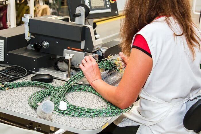 Today electronic manufacturers are quickly making use of different types of PCB circuits for their various electronic devices. In fact, printed circuit boards help to join different electronic components together with the help of cable assembly. Rigid-Flex PCB versus Rigid PCB and Cable assembly all are useful in various electronic devices.
An introduction to rigid and flexible sheet materials and their capacityIn fact, there is also a huge range of different printed circuit boards. So you have many choices in the selection of printed circuit boards for your electronics. In addition, each type has its own specific characteristics that are useful for different devices. The rigid plates are well known. Different entrepreneurs usually use rigid circuits. They actually think that rigid plates are much more expensive compared to rigid circuits. In addition, they also believe that rigid-flex boards are made by using flexible materials that are very expensive. But the truth is, flex circuits can offer great versatility and countless advantages over rigid boards. These assemblies are extremely convenient to use in mass production. Because they can save your valuable time during the assembly of the total machine. Moreover, the cable assembly manufacturers are increasingly using them in the automotive industry. We are sure that you have all the essential information about Rigid-Flex PCB vs. Rigid PCB and cable assembly. So let's take a look at the 4 reasons to use Rigid-flex boards instead of Rigid PCB boards and cable assemblies. Why Flex circuits are best in Rigid-Flex PCB vs Rigid PCB and cable assembly?In fact, there are several reasons for electronic designers to use Rigid-flex printed circuit boards instead of Rigid boards. We have listed 4 top reasons for you. these are:
Products that ideally use flexible circuits in Rigid-Flex PCB versus Rigid PCB and cable assembly As we have already explained to you flexible circuits are very beneficial to use in modern smart electronic devices. In addition, they are also perfect for use in the following products that require:
In which applications can Rigid-Flex printed circuit boards excel?The fact is that rigid-flex PCBs can be relatively more expensive compared to the rigid boards. But their durability, weight savings, compact size, reliability and several other benefits make them an ideal choice. In addition, all these useful features score them high in Rigid-Flex PCB vs. Rigid PCB and Cable Assembly. Today, electronic engineers rely heavily on them as these cards can surpass any other good electronic engineering. They have indescribable benefits, so electronic designers always prefer to use them. Moreover, they have the best ability to provide ideal benefits not only for rigid but also for flexible printed circuit boards. Here we have tried to put all those applications where rigid-flex PCB printed circuit boards excel. These extremely useful applications are: Higher- D certainty A applications: In fact, it sometimes becomes impossible to accommodate cable assemblies and connectors in just one small housing. Actually, all these connectors and cables are the essential need in such applications. Moreover, they are part of it. Rigid-flex circuits thus have the ability to fold all those necessary elements into very small profiles. These printed circuit boards save space and are best used in all of the above conditions. Very R reliable A applications: The Rigid-flex printed circuit boards are ideal for those applications dealing with extreme shocks or repeated vibrations. Because in such conditions, cable assemblies and rigid plates fail. Thus, electronic engineers rely heavily on rigid-flex boards in those applications where shock and vibration occur again and again. Hence, this is the reason why electronic designers prefer Rigid-flex boards in Rigid-Flex PCBs over Rigid PCB and Cable Assembly. Five or M ore R igid printed circuit board C, live circuit B oards: The engineers also make use of these circuits when they need to use five or more rigid boards. In addition, there are also cables to connect these rigid plates. All these factors make electronic solutions more complex. In such circumstances, rigid-flex boards are cost effective and an optimal choice. How do Rigid-Flex boards ensure highly effective, cable-free electronic designs?the ability to eliminate
They also make the design simple by reducing or completely eliminating the flexible cables and connectors. As well as, these boards also have the ability to provide electronic designers with an improved and reliable solution. Rigid-Flex PCBs Deal for high temperature applications in Rigid-Flex PCB versus Rigid PCB and cable assemblyIn this modern era of electronic technology, electronic manufacturers prefer to use rigid-flex printed circuit boards. They use these plates not only for manufacturing and consumer applications, but also in industrial devices. Because these circuits are very chemical resistant. In addition, these rigid flex plates are also resistant to exposure to high heat, UV radiation and radiation. In fact, PCB designers use the best quality polymer or polyimide (polyimide is almost like polymer). Therefore, these circuits can dissipate the extra heat relatively better than that of rigid plates. Their material is much better compared to rigid printed circuit boards. In addition, the best variation of polymer can also come under extreme conditions without negative effects. For example, the rigid-flex PCBs are ideal for use in industrial sensor technologies. So all these best features make rigid-flex circuits better in Rigid-Flex PCB vs. Rigid PCB and Cable Assembly. Why choose ideal material for rigid flexible circuits in Rigid-Flex PCB vs Rigid PCB and cable assembly?In fact, rigid-flex printed circuit boards work using the 2 most common and useful materials. These materials are:
Furthermore, you only need a very small amount of copper to make a rigid flexible circuit board and various other types of circuits. Polyimide glue:In fact, polyimide adhesive is the second worldwide material. This is very essential for use in rigid-flex circuits. Because it merges the rigid and flexible layers into a rigid flexible circuit board. In addition, electronics manufacturers need to practice a little before using polyimide adhesive in the rigid-flex board. Actually, it is essential to become an expert to use the polyimide glue. Otherwise you cannot construct an ideal working rigid-flex PCB. What are the popular uses of Rigid-Flex printed circuit boards?We realize that rigid-flex PCBs are more reliable when we talk about Rigid-Flex PCB vs Rigid PCB and cable assembly. They have countless uses in various types of modern electronic accessories. A very popular example of their application are smartphones. Today you see that modernist smartphones are more functional and extremely thin. All this has only become possible thanks to the latest rigid-flex technology. In addition, all modern computer electronics quickly make use of rigid-flex boards. You can see the latest electronic gadgets have gotten smaller like never before. All this progress has happened only because of rigid flex circuits. conclusion: We have actually tried to summarize all the useful applications of rigid-flex boards in modern electronics. Their applications are very extensive. As well as their implementation is growing more than your imagination. They are very effective to use in,
PcBA storage conditions are as follows:
One, avoid paint spray three For the pcb board assembly not being used for a long time, it should be coated with a three-proof paint, which has the functions of moisture-proof, dust-proof and anti-oxidation, and can effectively extend the storage time. After being coated with a three-proof paint, it can be extended for up to 9 months. II. Vacuum packaging method PCBA storage is not in contact with air and water. First of all, the PCBA board should be packed with vacuum bags and a layer of bubble wrap should be placed on the side of the box during packing. Bubble film has good water absorption, which plays a very good role in preventing moisture. Of course moisture resistant beads are also indispensable. Then sort them and label them. After sealing, the boxes should be kept in a dry and ventilated place out of the ground and away from sunlight. Get more Box Build Assembly Control the temperature and humidity of the warehouse The temperature of the warehouse stored by PCBA is best controlled at 23 ± 3 ° C and 55 ± 10% RH. The storage condition is good and the temperature is less than 25 ° C and the relative humidity is less than 65%. It has temperature control, and the inner environment is non-corrosive gas. Relaed post: https://theabsolutepcba.tumblr.com/post/642031620019339264/all-usb-cables-for-your-smartphone-and-computer https://absolutepcb.blogspot.com/2021/01/what-is-electrical-circuit.html https://absolutepcb.hatenablog.com/entry/2021/01/13/000000 https://absolutepcb.mystrikingly.com/blog/how-to-reduce-the-appearance-of-pewter-beads-in-pcba-production Anyone who ever does something with electronics has to get started with the soldering iron at some point. Based on examples on the internet, you can safely say that the soldering skills of the average tinkerer are not doing well. It would be a shame if your soldered project does not work properly due to small soldering errors. That could be better! We give 13 tips for soldering your own tech. Thanks to the popularity of boards such as the Raspberry Pi and the Arduino , tinkering with electronics still remains a popular activity for many. The components cost next to nothing, and diagrams and even complete project descriptions are eagerly exchanged on the Internet. If you get stuck with something, there are countless forums with helpful types who are eager to share their knowledge and skills with you. In short, it is a great time for electronics hobbyists. 01 Think of it yourself or reuse it? At the start of such a project, you are immediately faced with the choice of whether you have to devise the circuit yourself or if someone has already invented it. In the vast majority of cases, you can reuse someone else's work with some adjustments. For the necessary adjustments and for projects that you have to build from scratch, the breadboard is an indispensable tool. Stick the components in, connect them with jumper wires and you have a first version of the circuit in a few minutes. Because the code in many cases makes components superfluous - think of combinations of capacitors and resistors for oscillators and timers - circuits are becoming simpler and errors are more likely to occur in the code than in the hardware. When the stuff is on the breadboard, most of the time goes into debugging the code. And once the software works, the basics of the electronic part of the project is finished. Get more pcb assembly rework That's when the real work can begin: installing the circuit, so that your project can actually be used. Moving the components from the breadboard to a printed circuit board is the next step. 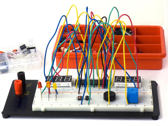 01 Before soldering, work out your entire project on a breadboard. 02 Experiment PCB For most measuring and control circuits, an experimental PCB is sufficient (also called protoboard or stripboard). Much cheaper and it saves designing a printed circuit board layout yourself, which is too difficult a step for the hobbyist. When choosing the most suitable plate, the dimensions are not even the most important: PCB material is easy to cut to size with a hacksaw. Much more important is the way in which the copper strips are distributed on the printed circuit board. These vary from only single islands to full length strips. A matter of taste, but we find pictures with groups of interconnected islands ideal, Costs: depending on the size, less than one euro to about ten euros. 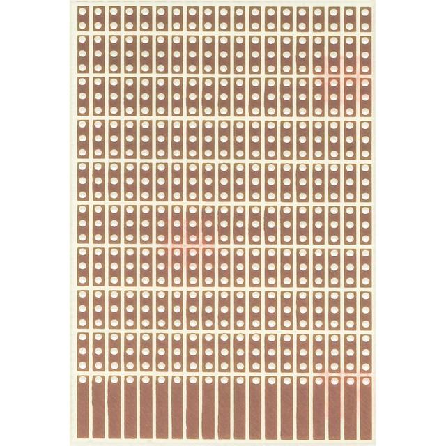 02 On an experimental board, groups of islands offer the most flexibility. Here a picture of 5 by 8 centimeters for two euros. 03 Assembling A corruption of the German bestücken (provided with) is used to place the components: pieces. Unlike industrial series production, hobbyists usually involve components whose legs or pins pass through the printed circuit board to solder them at the bottom. In the 1990s, the industry switched to smd components (surface-mounted devices), which are much smaller and are installed fully automatically (see box 'Surface-mounted devices'). With experimental printed circuit boards you have to think carefully about the location of the components when assembling. Logically, it is better to place parts that have many connections between them. The installation itself is a painstaking job. It is most efficient to apply all components first and then solder. That may seem difficult, because to solder you have to hold the printed circuit board upside down and without measures the components will fall off the printed circuit board. To prevent this, bend at least two protruding legs of each component that you apply, in opposite directions. That way, that component gets stuck when you turn the printed circuit board over. Use a small side cutter to cut the ends of all (including the non-bent) legs to a length of about two millimeters. Then place the next component and so on. When placing each component, make sure that all legs or pins are on their own island, otherwise you will connect them together. Integrated circuits and controllers can therefore often only be installed in one way: across the width of the PCB. Also visit pcb assembly manufacturer 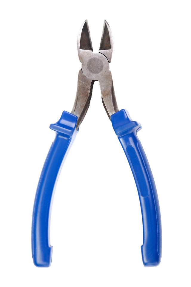 03 Side cutters are an indispensable tool for assembling a printed circuit board. Surface-mounted devices A separate category of parts are the smd components. These 'surface-mounted devices' have only tin-plated ends or very small legs and are soldered on the side on which they sit on the PCB. This is different from the traditional components whose legs go through the printed circuit board and which are soldered at the bottom. Hand soldering of smd parts is for advanced users, smd components are therefore not intended for that; one of the advantages is that they can be applied and soldered fully automatically by robots. 04 Which soldering iron? The most important tool is of course the soldering iron. The price varies from ten euros to hundreds of euros, the latter group being absolutely too expensive to use for hobby projects. These are soldering stations that can be set precisely to the degree and that is a great exaggeration for this manual work. You can work fine with a soldering station of a few tens. At Conrad you can already find nice models for around 25 euros. Such a station consists of a power supply, the temperature control and a holder for the soldering iron. A separate soldering iron is not recommended, unless you think it is a good idea to have a piece of metal on your desk that is close to 400 degrees. Always place it in a holder, which also offers space for a damp sponge, on which you can wipe the soldering tip clean. 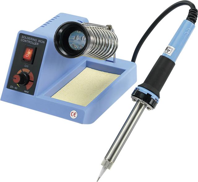 04 You can work fine with an affordable soldering station for around 25 euros. 05 Quality soldering tip The soldering tip is the part with which you actually solder and that is therefore decisive for the quality of the soldering iron. The composition and the associated hardness of the material determine the heat transfer of the post. And how long it will last, because corrosion is always lurking in a hostile environment of molten tin and highly variable temperatures. The shape is also important: for fine electronics, the rough tip of a typical hardware store bolt is of little use. For electronics there is a wide selection, ranging from chisel or screwdriver model to a cone-shaped tip in various lengths. The choice of pen depends on the specific application, a steady hand and personal preference. Do check out Cable and Wire Harness Assembly 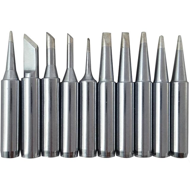 05 Soldering tips come in many types.
Use a soldering iron of at least 30 watts, even for fine electronics. 06 Temperature A second quality criterion is the heating element and specifically its power. To prevent the solder from melting properly or from solidifying too early, the temperature of the tip must not drop too much during soldering. Due to the much lower temperature of the parts to be soldered (room temperature), the temperature of the pen drops sharply as soon as you hold it against the parts and the heating element should be able to compensate for that immediately. For that reason, use a soldering iron of at least 30 watts, even for fine electronics. That is also the reason for choosing a temperature-controlled soldering iron: above 400 degrees most parts quickly break, so a heating element must be switched off when a certain temperature is reached. 07 Solder tin: lead or not? Until just over ten years ago, everyone used an alloy of lead and tin to solder electronics. Since 2006, lead solder has been banned from equipment sold within the EU. For health reasons it is recommended to also work with lead-free solder, which consists of alloys of tin and copper and / or silver. The disadvantage of the lead-free alternatives is a higher melting point and dull connections. That means soldering at slightly (about 40 degrees) higher temperatures, so a slightly higher risk of damage to sensitive components. More importantly, it is more difficult to determine the quality of the connection, a dull connection is an indication of a bad weld with lead-tin solder. Those who want to solder with lead-tin can still buy it. Related post: https://theabsolutepcba.tumblr.com/post/638953733112381440/circuit-boards-so-important-but-so-undervalued https://absolutepcb.blogspot.com/2020/12/how-to-add-simple-circuit-to-your.html https://absolutepcb.hatenablog.com/entry/2020/12/10/000000 https://absolutepcb.mystrikingly.com/blog/how-to-select-cables-and-connectors-for-your-application To optimize communication with customers, Eurocircuits has developed a third module, the PCB Configurator. The first module was the PCB Visualizer that reads the customer data, visualizes the print and indicates whether the data and the order details match. Module 2, the PCB Checker, goes a step further and analyzes the possible deviations in detail and indicates point by point, both visually and in value, what the deviation is.
PCB Configurator fills in the need to be able to change and recalculate things and also forms the basis for a new calculation tool. The advantage here is that the pcb assembly rework Configurator immediately validates any input or choice of technical or volume parameters and calculates a price. PCB Configurator also indicates which choices or combinations are impossible or lead to a serious price increase. The customer can also choose whether he wishes to use a straightforward html calculator or the more sophisticated PCB Visualizer software that is available after reading the customer data. Get more pcb box build assembly services In addition to the validations, PCB Configurator also contains a handy visually presented build-up configurator, and even in the html version a schematic representation of the chosen technical options for the PCB. The new calculation tool also offers an intelligent matrix with prices and delivery times. For example, the calculator not only shows the price for the selected quantity and delivery period, but also shows all meaningful more favorable quantities and delivery times. In this way, the customer has a faster insight into what the best order option could be for him. Related post: https://absoluteelectronics.dreamwidth.org/321.html https://absolutepcb.blogspot.com/2020/11/the-beauty-of-four-layer-pcbs.html https://absolutepcb.hatenablog.com/entry/how-is-a-pcb-manufactured https://absolutepcb.mystrikingly.com/blog/these-12-points-should-not-be-missing-from-the-sla-with-your-pcba-supplier  Every PCB (A) is different
PCB (A) stands for Printed Circuit Board Assembly. This is not just the bare circuit board, but the fully assembled product. Which factors determine the cost of a PCB (A)? Every PCB (A) is different and the requirements on the part of you as a client also play a major role. The factors below play the largest role in the cost of PCBA development : 1. Requested delivery time The shorter the delivery time, the higher the costs. The delivery time for a printed circuit board is a maximum of 4 weeks. The fully finished newly developed PCBA has an average delivery time of 1-3 months. This depends on the complexity. 2. Complexity and specifications of the print The more complex the specifications, the higher the costs. From simple PCBs with a few components to advanced PCBs that require software to be written. This includes:
3. Number of layers With printed circuit boards you have inner layers and outer layers . The more layers, the higher the costs. The possibility to mount parts on both sides also has an effect on the cost of the PCB Assembly. You can also give the PCB a protective coating. This coating can be both dust-repellent and / or waterproof. This depends on what the situation requires. Read more pcb prototype assembly service Size of the first and future order (s) Of course we take your budget and the future into account! The lower the order, the higher the price. The production price per PCBA is, however, lower as the order size increases. In addition, it is cheaper to order one annual order instead of five partial orders. We think along with you from idea to end product. This is reflected in a cooperation agreement. Purchase PCB production from Absolute PCB Assembly We have over 30 years of PCB assembling experience. From unique copies to batches of 100,000 copies. Our production department consists of fully automatic pick and place machines. These machines together have a capacity of more than 45,000 components per hour. Thanks to this capacity, we can offer you a fast delivery time at an attractive price. Related post: https://absolutepcb.blogspot.com/2020/10/what-is-embedded-system.html https://absolutepcb.hatenablog.com/entry/the-biggest-mistakes-new-makers-make https://absolutepcb.mystrikingly.com/blog/how-fast-can-a-pcb-a-be-delivered A box build, also known as systems integration, is an electromechanical assembly process that includes enclosure fabrication, installation and routing of cable harnesses, and installation of sub-assemblies and components. You can say that box build is a printed circuit board assembly in a big cabinet full of wires, or a complex fully integrated electromechanical system with pneumatics and electronics. Reference
Box build assembly services include system level assembly, product assembly, and sub-level product assembly. It also includes packaging, labeling, testing, software loading, product configuration, warehousing, order fulfillment, aftermarket service, and repairing. If you are considering a box build assembly process, you need to keep a few things in mind. You need to provide the following information and discuss with your assembly services provider so that they can serve you better. Bill of materials One of the most important requirements for any electronic manufacturing services provider – the bill of materials – will help get an idea of all the key components and materials that need to be sourced. Along with this list, you can also define the smaller elements like wires, nuts and bolts, adhesives, tie wraps, heat shrink, washers, etc. Although these elements are considered as consumables, they still have a price that you need to pay for buying. So, you must define them to avoid unexpected cost additions. Defining them will also prevent any kind of unpredicted production delays. 3D CAD model Provide a 3D CAD model so that the final product can be better visualized. A number of CAD packages are available today that offer free drawing viewers. With these packages, you can easily convert drawings into build instructions. A layout drawing with all the key components labeled with complete required information is essential. Dimensions Inform your provider about the size and weight of your required unit. This information will also help you decide on various factors like handling, storage, shipping, and every other process related to the build process. (You can also decide and inform your provider with the kind of packaging and transportation you require for your finished product.) Sample unit A sample unit is an important source of data in case of unfinished drawings. Having a sample unit is definitely helpful to make things easier. Your provider can help you plan and create drawings to guarantee reliable builds. Testing Safety is one of the prime concerns for any electrical device. So, for this electrical system of box build assemblies also, you need to specify the basic electrical safety testing like earth bonding and flash tests. Whatever you wish to perform – functional testing, factory acceptance testing, visual inspection, etc. – you must get into a discussion with your provider who can advice you with their knowledge and experience of what works best. Read more: pcb assembly usa So, be acquainted with all these decisions and information beforehand. Whether simple or complex, whenever you decide on having a box build assembly process, keep all this data in hand and discuss with your provider to get the best results. Miracle Electronics is a provider dedicated to lean manufacturing techniques in all operations and processes. You can get the best electronic box assemblies in India here, manufactured with maximum efficiency and constantly improved processes through highly knowledgeable and experienced professionals. |
Photo used under Creative Commons from wuestenigel
